As the size of devices that access the internet shrink, many new opportunities arise. Products such as Google Home Mini and Alexa are groundbreaking devices that change the way we interact with the internet. Mobile phones are also getting better and smaller. They are starting to think for themselves with Artificial Intelligence. Instead of typing questions we have into a traditional computer or phone internet browser, we are now asking devices things with our voice. Complete purchasing systems are now integrated into Amazons Alexa and anything on the internet is available to buy with a simple voice command. Google Home allows anyone to instantly access the internet to find information about traffic, news, movies, music, and the like. But with such potential also comes great security concerns. It is crucial to keep payments secure and anonymous to protect the privacy and assets of the user. Just in the past few years many companies have fallen to hackers and consequentially lost massive amounts of money. With the massive data breach of the well-known company Yahoo, in 2013 it was estimated that there was a loss of three-hundred and fifty million dollars from Yahoos sale price. Another such data breach impacted the online buying and selling site eBay, and it was estimated that it exposed confidential information of nearly 145 million users. Not only is strong passwords and encryption necessary, but it is also critical that information is transferred and stored securely. When internet encryption first came out, many websites used a standard for storing passwords known as MD5. However, this standard was not fully thought out and was soon cracked and completely insecure. Most all websites are now moving on to encryptions standards such as SHA254 which would take completely unreasonable amounts of time for even the best computers to crack. But that is just the information on the storage side. It is also critical to make sure when buying products online that the websites transfer payment information over protocols secured with SSL. Many people have fallen to the consequences of buying things off non-secure webpages, and that is why is so important that the public should be educated about internet security. Having managed a couple of websites myself, I have seen first hand the effects of not having the proper security built it. Once a website I was working on was compromised by a hacker because the proper SSL was not in place yet. The process of re-securing the website was quite difficult and took up a lot of time that could have been better spent else ware. In closing, the future of internet capable devices is quite bright, but developers should keep a close eye on the aspect of security to prevent future mishaps.
Smart Watch Project
So with summer approaching, I needed a project to keep me busy. I knew I wanted to build something small and reasonably cheap, that I could finish before summer ends. I decided to make a Smart Watch with a target price around $100.
I started looking around for other smart watch builds for examples, since I was having a hard time finding the right parts for mine (finding the right size of display was the main problem). I came upon this build: http://jared.geek.nz/2014/jul/oled-watch-is-alive. It was built very well, so I kind of used it as a guidebook as I went along with this project. This project is in no way a direct port of that project, but it does have a few similarities, as I used the same battery charger as he did and a similar screen - But that’s about it.
Next step: Design. The schematic for the project can be found here: https://github.com/Supercap2F/Smart-Watch/blob/master/KiCAD/SmartWatch.pdf. The processor for the watch is a 32-bit PIC microcontroller (PIC32MX370F512). The screen is a 128x128 OLED bought from buydisplays.com. I also designed in a 6-axis accelerometer/magnetometer (FXOS8700CQ) and a FT201X for USB communication. The battery is a 150mA LiPoly off of ebay. I didn’t design in any bluetooth or wifi functions because I don’t know much about RF stuff and space is quite limited.
Here’s the PCB design (it’s four layers in all):
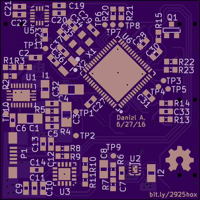

In total I think I spend about 7+ hours designing it. Towards the end I started to get scared I would run out of space to route the traces, but I was able to do it by routing a couple sort traces on the internal power plane. It’s a double-sided load so I’ll use a stencil for the top and hand solder the bottom.
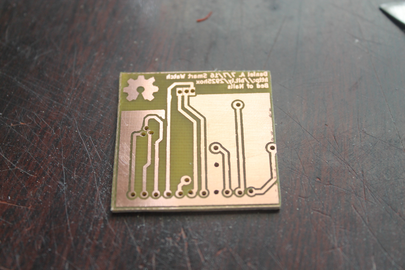
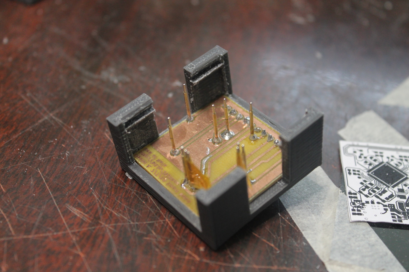
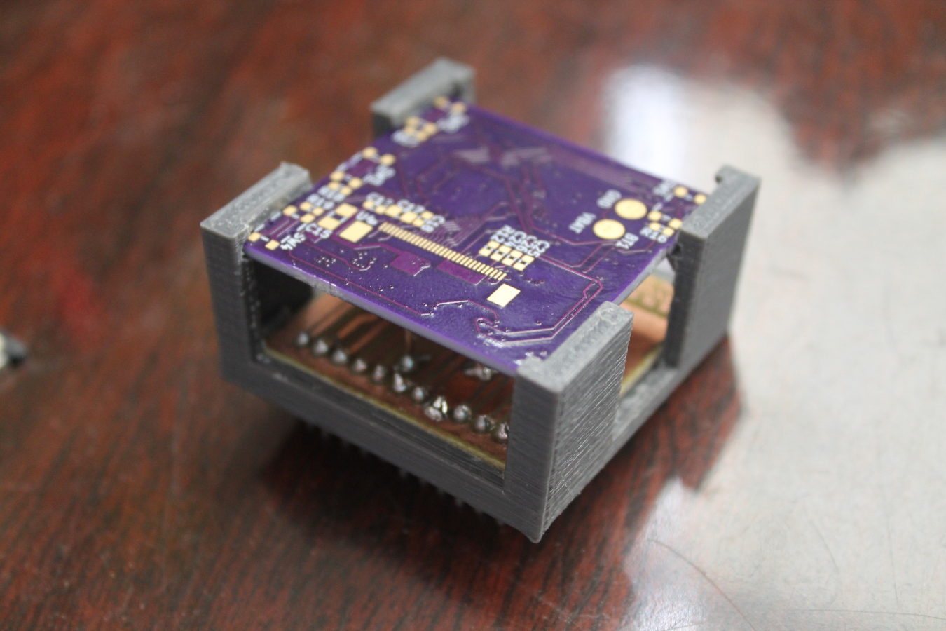
This is the programming jig (bed of nails) for the watch. I etched the PCB myself and the holder is 3D printed. I got the pogo pins off of ebay, 50 for 4 bucks - most likly not the best quality. I had to put some kapton tape between them so they wouldn’t short out.
Update on July 14th 2016
The PCBs came in! I did a dry fit for the jig:

It lined up fine after a little cutting on the jig holder.
So I applied solder paste to the PCB and started placing the components. I got about ten down when I found out that the pads for the battery charger where mirrored! *cries*
I think the reason that happened lies in the datasheet, they didn’t say what orientation the part was in in the pin numbering diagram. Granted, I should have realized that clockwise pin numbering is a little odd to say the least. Well there goes $40+ for the PCB and Stencil, plus the three-weeks it takes to get the board in. Looks like this might not get done before the end of summer after all. :(
Homemade PCBs with a Brother Printer - 4mil Traces
Homemade PCBs with a Brother Printer - 4mil Traces
So I’ve done a bunch of tests with different paper, and the best paper I found for the job was this yellow stuff off of ebay here. I think this is the key part to getting such good results.
It took a couple of tries to get the toner to stick to it, but in the end I got it working by taping a piece of it to some plan paper with kapton tape.
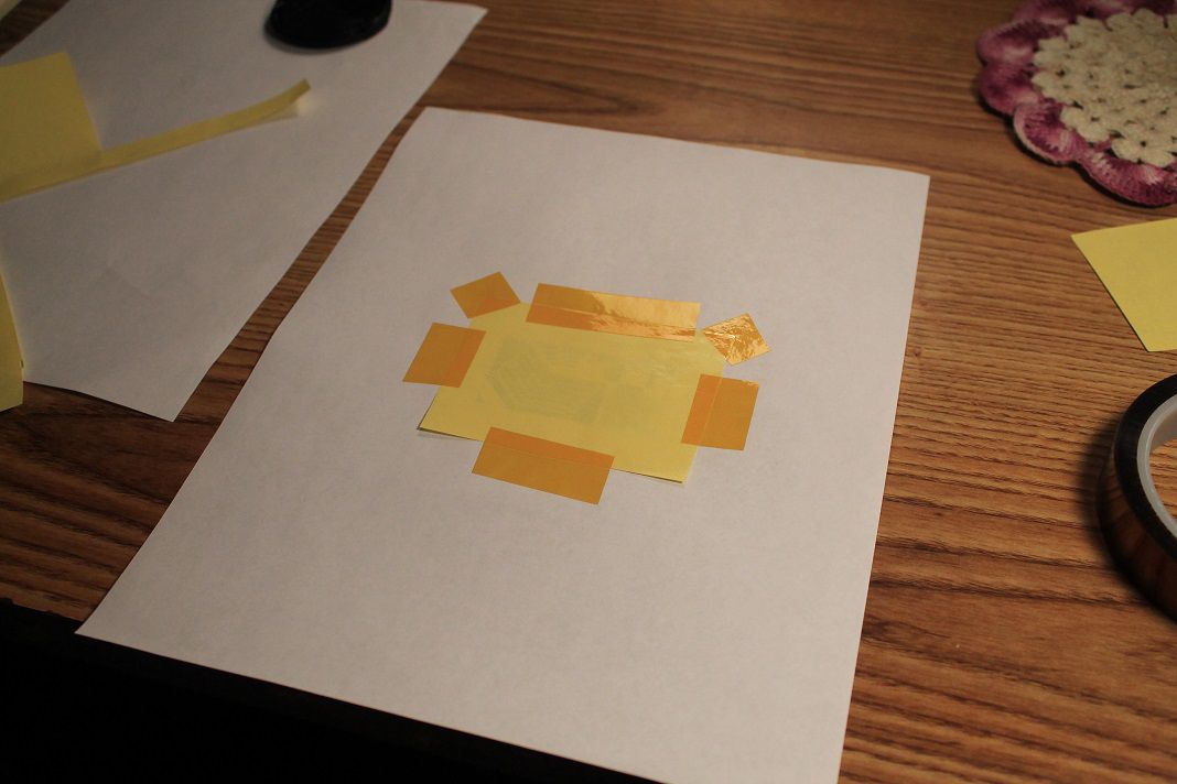
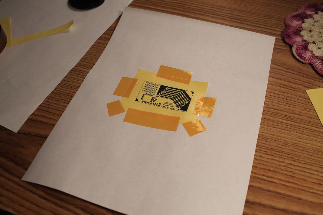
I use a pretty standard way of transferring the toner to the PCB. I just tape down the toner transfer paper to the PCB, put a paper towel over it, and iron it on (two minutes seems to work good). After the two minutes, I spray the towel and PCB with water and iron it out – I repeat that for about one minute.
After that I let the PCB cool, and wash off the toner paper in cool water.
For etching I use strait ferric chloride in a squarish plastic container. It usually takes about 20 minutes to etch if I agitate the container, or less if I rub the ferric chloride on the board:

I then rinse off the board in cold water again, and remove the toner with lacquer thinner or acetone. And that’s all!
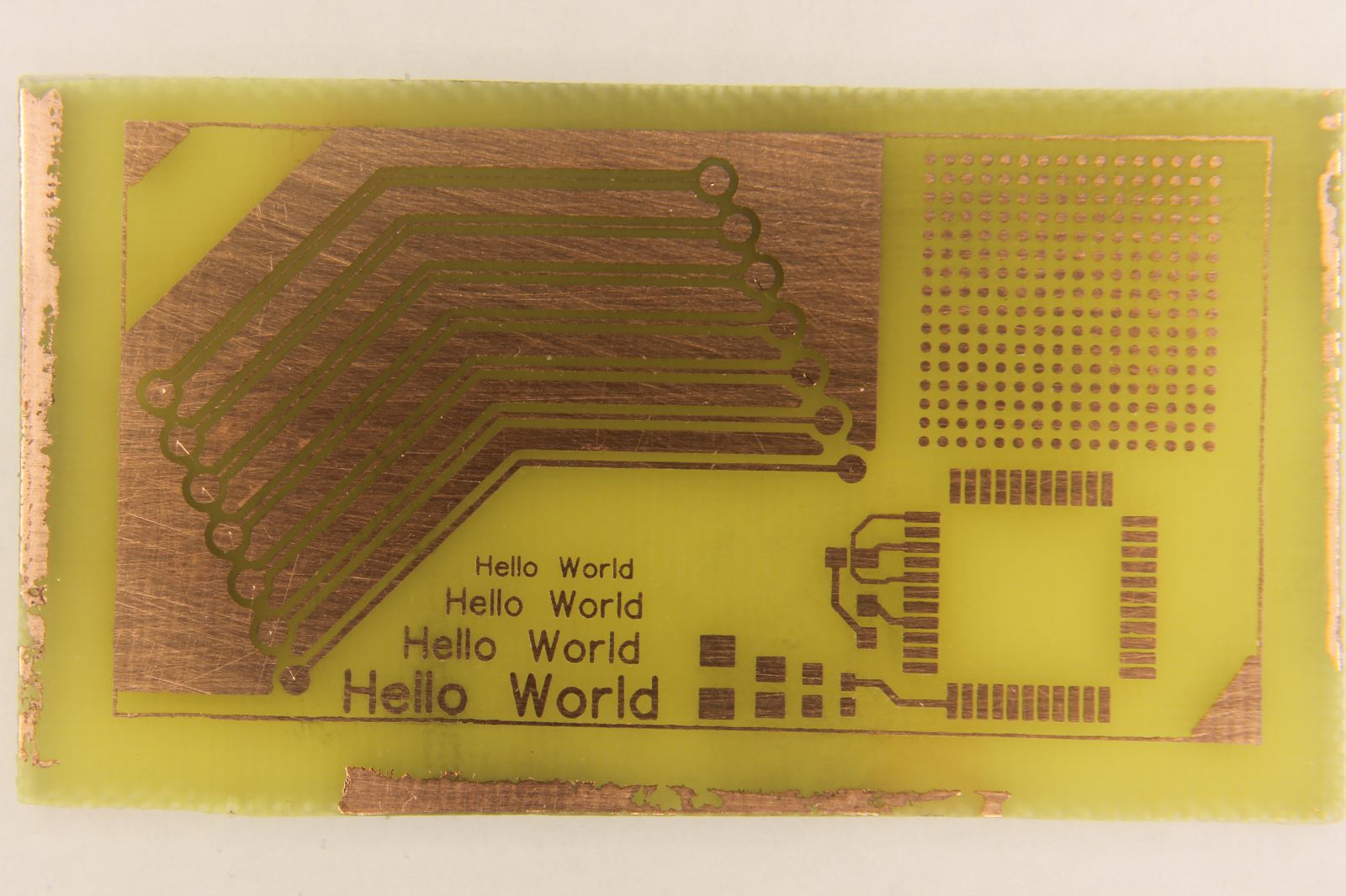
(The first trace on the top-left is 2 mil, and the next one is 4 mil)
With this method I have reliably got down to 4 mil traces - I did get a 2 mil trace, but it was starting to have higher resistance (I wouldn’t trust it at all)…
CPU Power Supply Mod
CPU Power Supply Mod
This project came out of wanting to etch my first useful PCB, as up to now all the PCBs I’ve made have been tests. I have a old CPU power supply thats been lying around for awhile, so I decided to convert it to a PSU I could use on my bench.
First I started googling around for info on it, and found that it uses a standard computer PSU pin-out called ATX 2.x. The wikipedia article on it is here.
The specifications for the power supply are as follows:
- +3.3VDC/17A
- +5VDC/22A
- +5VDC/2A (Standby)
- +12VDC/18A
- -12VDC/0.8A
- 300W Max power
I’m planing to make all the circuitry handle about 3A maximum current draw on each channel. I’m going to fuse it for 2.5A for now though. If I ever want to be able to draw more current then that, which is not likely, I guess will just have to modify it some more. :D
So to the first order of business - draw a schematic. Here it is:
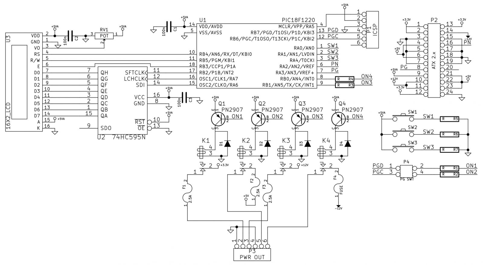
I decided to use a PIC18F1220 for this project because I have quite a few laying around. A 1602 LCD will be used for the user interface – I’ll need some way of telling the user which voltages are switched on. Three switches will work for user control (Select/up/down – or something like that).
P4 is a jumper, it connects PGD to ON1 and PGC to ON2, and is there for when the PIC is programmed. Since I ran out of I/Os I had to use the two pins that are for programming the PIC. And when the PIC is programmed I don’t want anything screwing up the communication between the computer and the PIC, so P4 should be unjumped while programming (is that even a word? :D).
Here’s the PCB layout:
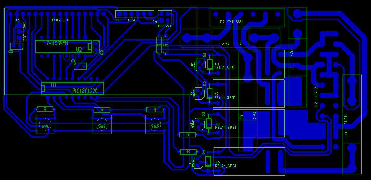
Yes, I know that the fuses overlap other parts - The plan is to have the fuses mounted on the back side of the circuit board and the rest of the parts on top. The relays are some high current ones that I salvaged from a used circuit board, I think they where out of a broken fryer to be exact.
Unfortunately, I will have to solder about eight jumper wires on where I couldn’t figure out how to run a trace, not shown here but they can be seen in the KiCAD file as un-routed traces. I guess I should have tried to optimize it a little more, but space was kind of lacking…
On to etching!
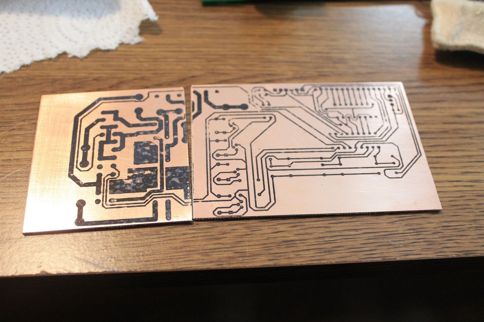
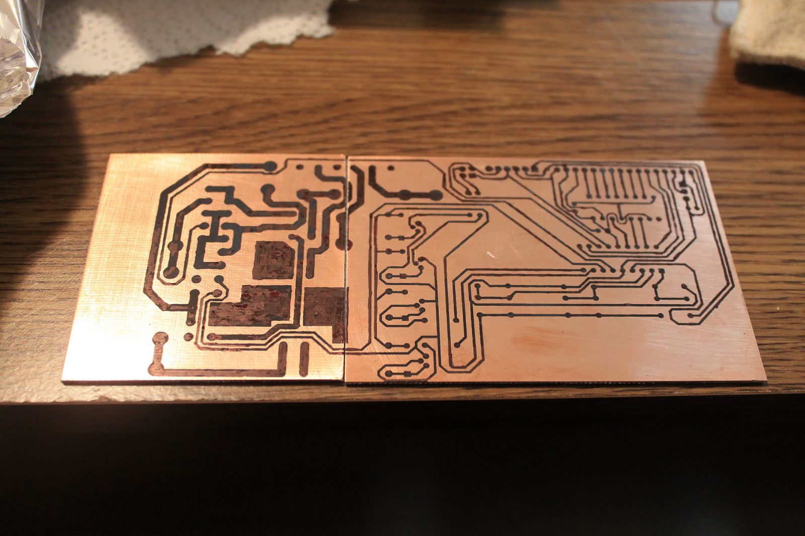
The first photo is right after the toner transfer. As you can see, there are quite a few spots where the toner did not stick ideally. The second photo is after touching up with a sharpie.
I think I may have rushed the toner transferring part a little, and that’s why it didn’t turn out so good. I could have redone it, but I didn’t want to use up any more of my all to little supply of glossy paper.
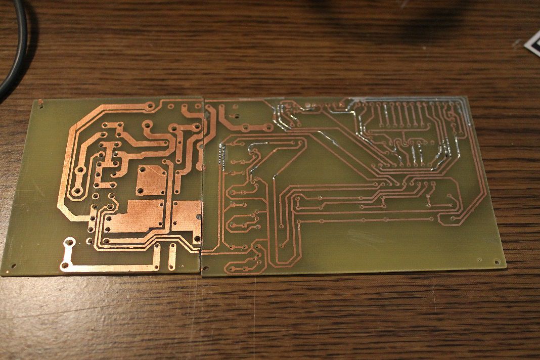
So after etching, I realized that sharpie is probably not the best resist. It appeared that some had come off during the process… Here’s a photo of the PCB after patching the broken traces with solder (sorry I forgot to take a photo right after etching):

The next step will be drilling the holes on the PCB. But unfortunately my drill bits haven’t arrived yet, so I will just have to call it for now.
Update on 10/7/15
The drill bit’s came in!
I also decided to try and put a silkscreen on the board.
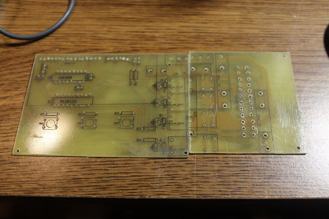
I used the same method as I did for the copper side. But as you can see, on the right side of the left board the transfer moved and blurred out. It doesn’t really matter much though, as this was more of a test to see if I could do it, and also the relays will cover it up.
Next step - Soldering!
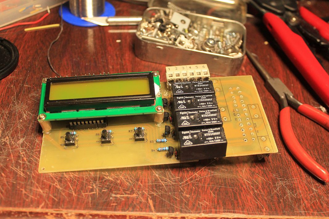
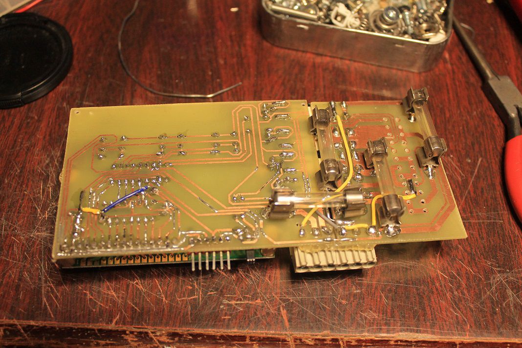
Everything soldered up pretty nicely. I used stranded wires for the LCD connections so it could be pulled backwards if I need to get at the parts under it. I decided to mount a switch instead of a jumper on P4, which should make it a little less painful to program it.
Everything was going good until I realized that somewhere along the line the connector for the power supply got mirrored on the PCB! I guess I will just have to hand wire it. *cries*
Update on 10/13/15
So I opened up the power supply case to cut out some wires that I don’t need for this project, and looky what I found:
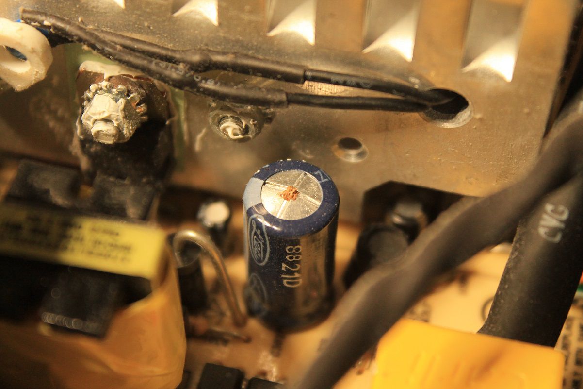
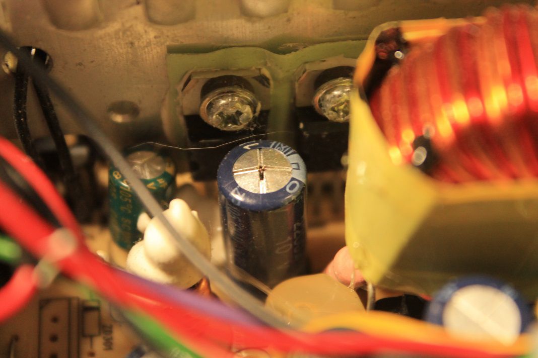
I think this power supply has had a lot of hours running. As I remember though, the computer I pulled it from still worked, so I think I will just over look that for now.
Next I made a chassis out of the metal from an old popcorn can (it’s tin so it solders nicely), and attached the circuit board to the power supply.
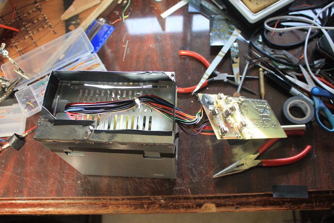
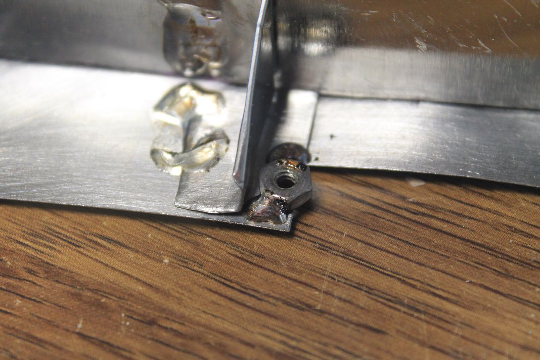
Photo two is a nut I soldered to the chassis so I could attach the circuit board to it with screws (aka make it easy to take apart and troubleshoot when it doesn’t work - lol!). I had to get out the weller 140W soldering gun to make the joints, as my regular soldering iron just couldn’t cut the mustard.
It lives!!

The display looks kind of weak, but it may just be a bad LCD.
Next step will be to write some code.
Update on 10/29/15
I guess the next step isn’t going to be writing code - instead it will be troubleshooting the PSU!
So after playing around with a little code, things just didn’t seam to be working right. I decided to check the standby voltage, and to my great surprise it read about 2.8VDC, not 5V as expected! So I hooked it up to the scope (being careful to hook ground up in the right spot) and here’s what I got:
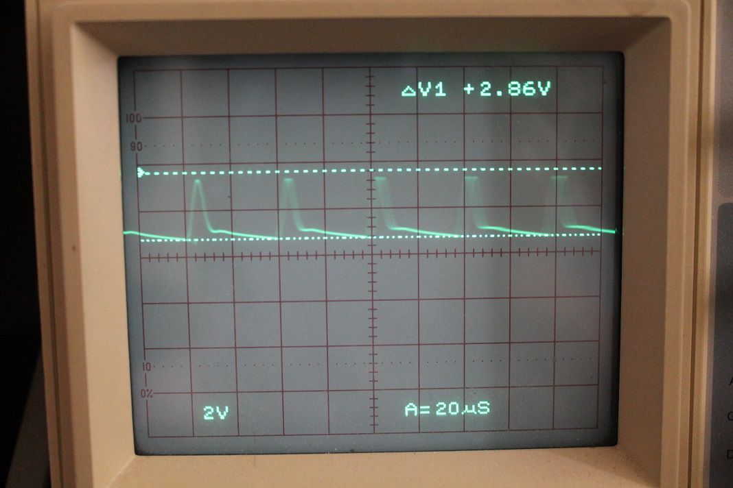
looks like the fault of a seriously bad capacitor to me! So I wrote down the values of all the caps that looked suspicious and bought some new ones from digikey (of much higher quality).
After putting the new caps in, I turned it on and the problem seamed to still be there… After some more experimenting I found out that all the screws that hold the PSU circuit board in place have to be in for the unit to work - they connect to the metal chassis completing the ground plane. It now works great! All the voltages are nice and flat, and the LCD works a lot better too.
Update on 11/14/2015
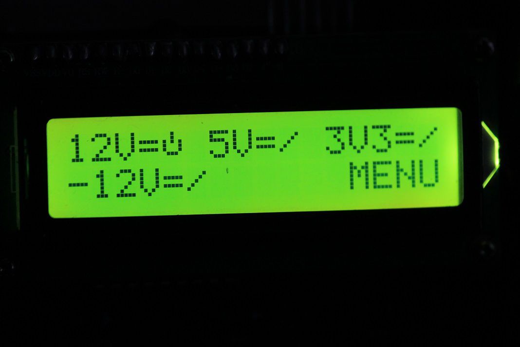
Well, I finished the code and posted it on github. Here’s a photo of the power supply’s main screen while running:
And the finished power supply above my desk:
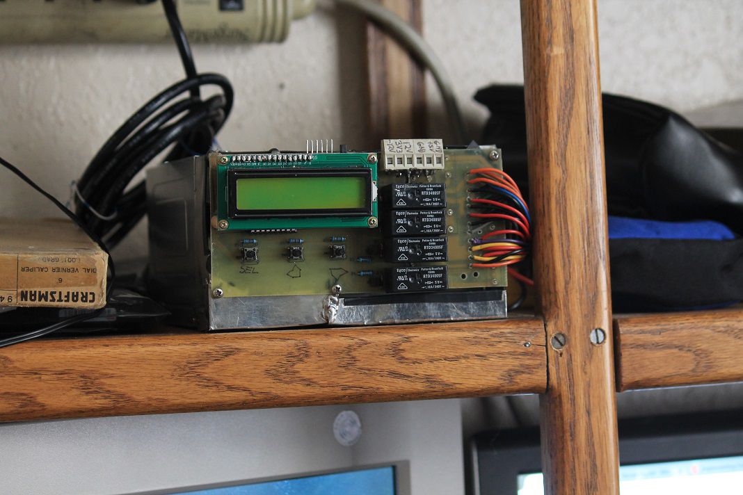
I’m pretty happy about how it turned out. It doesn’t look very good from the front though. I’ll probably end up making a cover for it some time in the future.
Update on 6/15/2016
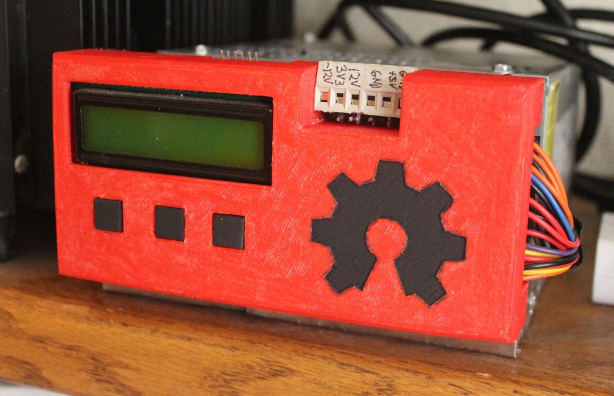
So I finally got around to making a front cover for the PSU. I recently acquired a 3D printer, so I thought I would finish up the project with a nice cover for the front. And with a little paint, it looks really nice:
